
Flip Flops
Contents
ToggleFlip-flops are sequential circuits, acting as precise 1-bit memory cells that capture and hold data on clock edges ( between the change of the value of clock pulse; b/w 0 and 1 or 1 and o) with two stable states that store a single bit of binary data, making them the basic building blocks of memory in digital systems.. Unlike level-sensitive latches, these edge-triggered wonders synchronize state changes, forming registers, counters, and state machines in CPUs, RAM, and gadgets worldwide. The operation of a latch can be modified by providing an additional control input and the latch along with that additional control input makes the Flip Flop.
Flip-flops are bistable circuits with clock (CLK) input, changing state only at rising/falling edges for glitch-free operation. It is a binary cell capable of storing 1 bit of information. It maintains it binary state until directed by a clock pulse to switch states. Built from latches, they store Q (output) and Q̅ (complement). Edge triggering ensures predictability in noisy environments.
A Flip Flop operates in two modes-
- Latch Mode – It is also known as the Hold Mode. The flip-flop stops following the input and stores the last value.
- Transparent Mode – In this mode, any change in input instantly appears at the internal output.
Core characteristics of Flip Flops
1. Two stable states: A flip-flop can hold one of two states, representing a binary 0 or 1.
2. Sequential circuit: Its output is dependent on the current state and previous inputs, unlike combinational circuits.
3. Clock signal sensitivity: Flip-flops are edge-sensitive, meaning their output only changes on the rising or falling edge of a clock pulse, providing predictable timing.
4. Data storage: They act as basic memory cells, capable of storing one bit of information.
5. Asynchronous inputs: Many flip-flops include asynchronous preset and clear (CLR) inputs that can override the clock signal to force the output to a specific state (1 or 0) without waiting for a clock edge.
How does a Flip Flop work ?
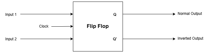
- Building the Memory: A flip-flop is built from logic gates (like NAND or NOR gates) arranged in a specific feedback structure (e.g., two cross-coupled latches).
- The Hold Mechanism: When the clock isn’t triggering, the gates keep the output Q stable, essentially creating a tiny loop that holds the current value.
- Storing the Bit: When the clock pulses (on its rising or falling edge), the input (like D, S, or R) is sampled and passed through the gates, forcing the Q output to either a ‘0’ or ‘1’.
- The Output (Q): This Q output is the bit of information being stored. It stays at that level (0 or 1) until the next clock pulse arrives and the gates reconfigure to store a new value
Purpose of Flip-Flops in Digital Systems
Flip-flops store bits temporarily, synchronize data across clock domains, and build complex logic like FSMs. They enable pipelining in CPUs, frequency division in clocks, and data shifting in comms. Without them, async chaos reigns—no reliable multitasking or memory.
In ALUs, they latch adder results; in RAM, arrays form words. Your CodeMirror compiler uses flip-flop sims for state verification.
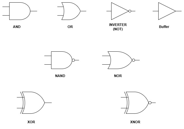
Types of Flip-Flops
Four core types dominate: SR, JK, D, T—all clocked, edge-triggered.
SR Flip-Flop: Basic Set-Reset with Clock – Has Set and Reset inputs; however, an indeterminate state occurs when both inputs are 1.
JK Flip-Flop: Versatile Toggle Master – An improvement on the SR flip-flop, it can be configured to set, reset, or toggle its state and has a predictable output even when both J and K inputs are high.
D Flip-Flop: Simple Data Capture King – Captures the value of the D (Data) input on the clock edge and holds it at the output until the next edge, eliminating the invalid states of SR flip-flops.
T Flip-Flop: Toggle Frequency Divider – A modification of the JK flip-flop where the T input determines whether the output will toggle or remain the same