SR Flip-Flop is the foundational clocked sequential circuit that stores one bit using Set (S) and Reset (R) inputs, synchronized by clock edges for precise state control. This edge-triggered evolution of the basic SR latch powers reset logic, registers, and counters in CPUs, making reliable memory possible in noisy digital environments.
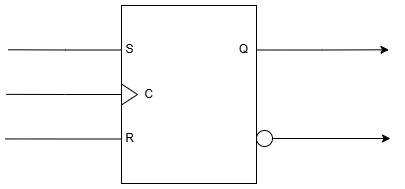
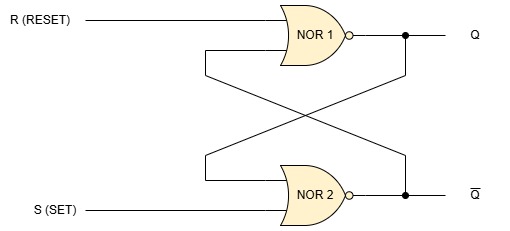
An SR Flip Flop has three inputs and two outputs. S(set) , R (reset) and C (Clock) are the 3 inputs and Q and Q̅ are the two outputs.
How does a SR Flip Flop work with Clock input in NAND SR Flip Flop ?
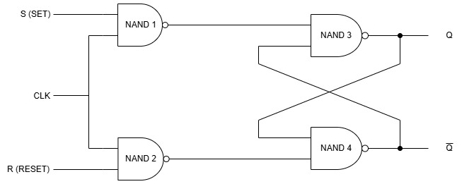
NAND based SR Flip Flop
A NAND based SR Flip Flop circuit is made up of two NAND gates and a NAND based SR Latch. The first two NAND Gates constitute the logic 1 part and the NAND based SR Latch constitute the second logic.
The S and R inputs works in the same manner as in SR Latch. But the SR Flip Flop does not respond to the inputs unless the edge of the clock signal rises. Whatever may be the values are at S and R, if the C input has no signal (C=0) then the output of the circuit cannot change. When the clock signal becomes 0 to 1 then the output of the circuit changes depending upon the inputs of S and R.
In the diagram of NAND based SR Flip Flop, the outputs of NAND gate 1 and NAND gate 2 stay in their logic as long as the clock input is 0. These outputs which inputs at the NAND based SR Latch holds their present state which means no change occurs. When Clock = 0, then present state = next state.
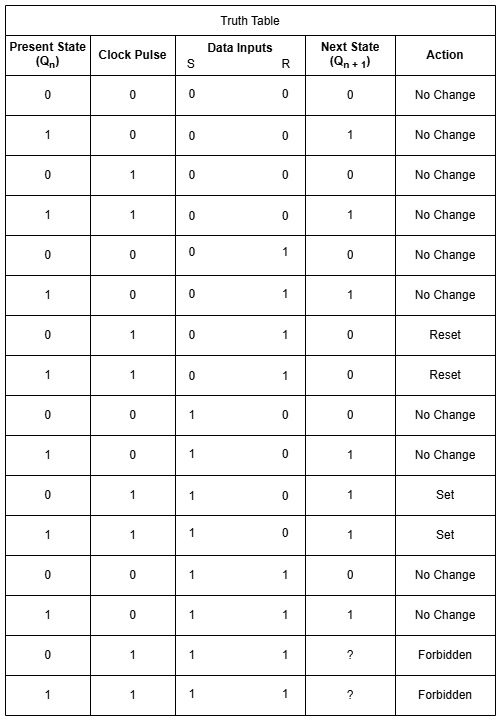
From the truth table of the NAND based SR Flip Flop total of four cases can be derived.
Case 1: When S =0 , R=0 and C=0, the flip flop stays in its present state. The value pf Q continues to be the same. Even when S=0,R=0 and C=1 (rising edge of the clock), the flip flop remains in the present state (Qn). The first four rows represent the unchanged state of the flip flop in any condition. (Qn =Qn + 1 ).
Case 2: When S=0 and R =1 and C =0, the flip flop remains in its present state. The value pf Q continues to be the same. But when S=0 and R =1 and C =1 (rising edge of the clock), the NAND gate 1 gives the output 1 and the NAND Gate 2 gives the output 0. Now the output 0 from NAND gate 2 goes to NAND gate 4 as input and gives the output Q̅ =1 which eventually gives Q =0 from NAND gate 3. So for S=0,R=1 and C=1 , the flip flop RESETS to 0.
Case 3: When S=1,R=0 and C=0, the flip flop remains in its present state. Again, the value pfQ continues to be the same. When S=1,R=0 and C=1, the NAND gate 1 outputs 0 and NAND gate 2 outputs 1. Thereafter, the output 0 from NAND gate 1 goes to NAND gate 3 to generate Q=1, which in turn generates Q̅=0 making the flip flop in SET state.
Case 4: In this case when S=1,R=1 and C=1, it ultimately results in Q=1 and Q̅=1 which is a forbidden condition.
Real-World Applications of SR Flip-Flop
Reset generators in CPUs (power-on clear). Switch debouncers (eliminate bounces). Frequency dividers (safe hold). Control signals in elevators (set floor state). UART start bits. Billions in ICs yearly. Ties to full adders: SR latches carry flags.
Limitations & Modern Mitigations
Forbidden state solved by preset/clear. D Flip-Flops replace in data paths. HDLs (Verilog) abstract issues.
Spread your knowledgeMultiplexers in Digital Electronics: Definition, Functions, Working & Truth Table Multiplexers, often called MUXes, are essential combinational circuits […]
Spread your knowledgeVon Neumann Architecture Explained Von Neumann Architecture forms the backbone of modern computers, storing both data and instructions […]