
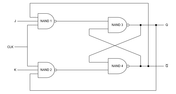
The JK Flip Flop is made from SR Flip Flop. It is 75% similar to a SR Flip Flop. A JK Flip Flop is build from an clocked SR Flip Flop. JK Flip Flop contains two inputs J and K with the clocked input. The input J along with the Q̅ output are applied to the first NAND gate which gives the output JQ̅. Similarly, the K input along with the Q output are applied to the second NAND gate which gives the output KQ.
The J and K input are equivalent to the S and R input of a SR Flip Flop respectively. When J=1 and K=1, the output of the JK Flip Flop toggles. Toggle means that it switches to a complement state. If previously Q was 0, then Q in the next state (Qn + 1) becomes 1 and vice versa.
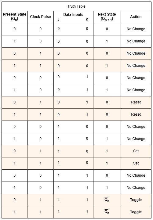
Lets say the previous values of Q and Q̅ are 1 and 0 respectively
Case 1: When J=0,K=0 with clock low, and whatever be the value for previous state, Q will hold the previous value. When J=0,K=0 with clock high and whatever be the previous value of Q (1/0) , the flip flop will hold its state. i.e (Qn = Qn + 1 ).
Case 2: When J =0,K=1, the first NAND gate receives 3 inputs (J=0,Q̅=0 and CLK=1). In NAND gate if one input is 0 then it forces its output to 1. So, JQ̅=1. Similarly, the second NAND gate receives 3 inputs (K=1,Q=1 and CLK=1)which forces its output to 0. So, KQ=0.
KQ=0 and Q=1 as inputs are applied to the fourth NAND gate which gives the output Q̅ as 1. Meanwhile , JQ̅=1 and Q̅=1 as inputs are applied to the third NAND gate which gives the output Q as 0. So, the next state is 0.
Case 3: When J=1 and K=0, the first NAND gate receives 3 inputs (J=1,Q̅=0 and CLK=1) and produces the output 1. So, JQ̅=1. Similarly, the second NAND gate receives 3 inputs (K=0,Q=1 and CLK=1)which forces its output to 1. So, KQ=1.
KQ=1 and Q=1 as inputs are applied to the fourth NAND gate which gives the output as 0. Alongside , JQ̅=1 and Q̅=0 as inputs are applied to the third NAND gate which gives the output Q as 1 making the next state as 1.
Case 4: In SR Flip Flop, when both inputs are 1 then the situation is forbidden. In JK Flip Flop when J=1 and K=1, the first NAND gate receives 3 inputs (J=1,Q̅=0 and CLK=1) and produces the output 1. So, JQ̅=1. Similarly, the second NAND gate receives 3 inputs (K=1,Q=1 and CLK=1)which forces its output to 0. So, KQ=0.
KQ=0 and Q=1 as inputs are applied to the fourth NAND gate which gives the output as 1. Alongside , JQ̅=1 and Q̅=1 as inputs are applied to the third NAND gate which gives the output Q as 0 making the next state as 1. This makes overcome the invalid/forbidden situation of SR Flip Flop and makes a toggle situation where the output switches from 1 to 0 and from 0 to 1 based on the input values.