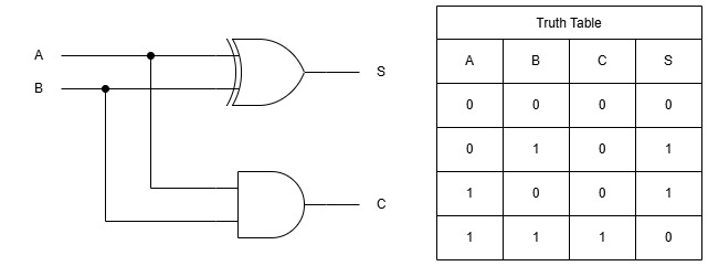

Latches vary by inputs and behavior, from basic SR to versatile D types. All use gates for feedback.
SR Latch: The Basic Set-Reset Building Block
SR (Set-Reset) latch uses two inputs: S and R and two outputs Q and Q’. These two outputs are complement to each other. Q is the stored bit in a latch.
An SR latch has two stable states:
Q = 1 and Q̅ = 0
Q = 0 and Q̅ = 1
Whichever value Q settles to, it stays there because of the feedback loop between the two gates. That stable output (Q) is the stored bit.
Why Q acts as memory?
The outputs are fed back into the inputs of the gates.
Because of this:
If Q becomes 1, the feedback keeps it 1 until an input forces it to change.
If Q becomes 0, the feedback keeps it 0 until an input forces it to change.
So the circuit remembers the most recent state. This is why it’s called a bistable device.
We don’t know initial Q, Q̅. At power-on, Q and Q̅ do not have predetermined values. There is no built-in memory of which side should start as 0 or 1.
Q and Q̅ depend on:
transistor mismatches
wiring delays
minute differences in voltage rise
noise
race conditions
So at the moment of powering up Q and Q̅ generally become random but complementary. The latch will quickly settle into one of the two stable states:
Q = 1, Q̅ = 0
orQ = 0, Q̅ = 1
The SR latch can be implemented by NOR and NAND gates.
i) NOR based SR Latch
A simple S–R latch (Set–Reset latch) can be built by connecting two NOR gates back-to-back so each gate’s output feeds one input of the other. That feedback path is why this is an asynchronous sequential circuit: the latch changes state immediately when inputs change (no clock).
The inputs are S (set) and R (reset) and the outputs are Q and Q̅ (the complement of Q).
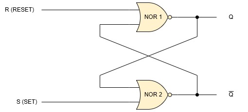
Functioning of an NOR based SR Latch
We know that the NOR gate only provides the output as 1 when both its inputs are 0. Otherwise if one its inputs are 1 then the output comes as 0. The NOR gate does not look for its other input when it gets one input as 1 and outputs 0.
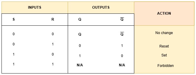
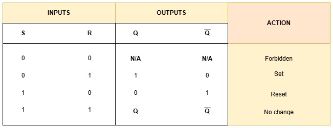
Case 1: S = 0, R = 0 (Hold State)
The first case where S=0 and R=0 is said to be in the hold state or in no change state. Both inputs are 0, so neither NOR gate is being forced. Each output is driven by the feedback from the other gate, so the latch simply remembers its previous state. If Q was 1 it stays 1; if Q was 0 it stays 0.
Case 2: S = 0, R = 1 (Reset)
In the second input condition, the R = 1 forces the output of the first NOR gate to 0 (Q=0). Q flows through the feedback path to the second NOR gate So, S=0 and Q=0 the second NOR produces Q̅=1.
With R = 1 and S = 0 the latch is forced to the reset state: Q = 0, Q̅ = 1. After R returns to 0, the feedback holds that reset state.
Case 3: S = 1, R = 0 (Set)
Symmetrically, S = 1 forces the second NOR that drives Q̅ to 0, which (via feedback) causes the other NOR to produce Q = 1. S = 1, R = 0 puts the latch into the set state: Q = 1, Q̅ = 0. When S returns to 0, the latch keeps that state.
Case 4: S = 1, R = 1 (Forbidden)
Both NOR outputs become 0 (because each NOR has at least one input = 1). So Q = 0 and Q̅ = 0 simultaneously, which violates the required complementarity (Q̅ should be the inverse of Q). When S and R later go back to 0, the feedback causes the two outputs to fight each other. The final state depends on tiny timing differences and is therefore indeterminate or metastable. For reliable operation, S and R should never be 1 at the same time.
ii) NAND based SR Latch
A simple S–R latch (Set–Reset latch) can be built by connecting two NOR gates back-to-back so each gate’s output feeds one input of the other. That feedback path is why this is an asynchronous sequential circuit: the latch changes state immediately when inputs change (no clock).
The inputs are S (set) and R (reset) and the outputs are Q and Q̅ (the complement of Q).
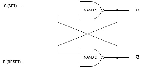
Functioning of an NAND based SR Latch
We know that the NAND gate only provides the output as 0 when both its inputs are 1. Otherwise if one its inputs are 0 then the output comes as 1. The NAND gate does not look for its other input when one of its input is 0 and outputs 0.
Case 1: S = 0, R = 0 (Forbidden)
The first case where S=0 and R=0 outputs Q=1 and Q̅=1. This condition is ambiguous and is said to be forbidden as latches outputs should be complement to each other.
Case 2: S = 0, R = 1 (set)
When S=0, the first NAND Gate forces the output Q=1. The second NAND gate that produces Q̅ as 0 takes inputs as R=1 and the feedback as Q=1.
With R = 1 (and S = 0) the latch is forced to the reset state: Q = 0, Q̅ = 1. After R returns to 0, the feedback holds that reset state.
Case 3: S = 1, R = 0 (Reset)
The condition S=1 and R=0 forces the lower NAND gate output to 1. So both the inputs of upper NAND gate 1 and therefore the output of upper NAND gate is LOW(Q=0). This condition resets the latch, i.e Q=0 and Q̅=1.
Case 4: S = 1, R = 1 (No Change)
The last condition S=1 and R=1 does not affect the state of the latch. It remains in its previous state.